Hard Materials

Carbon based Materials
This activity mainly deals with carbon-based nanostructured materials (nanotubes, nanodiamonds, nanographites), their synthesis, post-synthesis treatment, and structural, morphological, and functional characterization.
Part of the research is also dedicated to hybrid materials (carbon + metals, oxides, substrates) with applications in the energy, electronics, and sensor fields and, more recently, in the improvement of superconducting films.
Nanodiamond (NDs) are Nanoscale diamond particles that can be obtained through detonation (detonation nanodiamond) or chemical vapor deposition (CVD). They made of carbon in diamond form, with some defects, a modifiable surface, often oxidized or functionalized. They find large use as part of hybrid structures: nanodiamonds decorated with gold (Au) for imaging, biosensing, and plasmonic property applications. As a support in conductive nanocomposites (e.g., with PEDOT-type polymers) to improve hardness, stability, and conductivity. To improve the surfaces of YBa₂Cu₃O₇−δ (YBCO) superconducting films obtained by Chemical Solution Deposition: the addition of ND produces denser, smoother films with better grain connection, increasing the critical current density in zero field conditions.
NDs have high specific surface area and many reactive sites on the surface and find large applications for functionalization, for attaching other materials or functional groups. They have a good chemical and thermal stability, good hardness and high thermal conductivity but electrically insulating properties, unless modified. In superconducting applications, they influence film nucleation and growth: they promote more compact, smoother films and improve microstructure.
Carbon nanotubes are nanoscale graphite tubes, or rolled-up sheets of graphene. SWCNTs are thinner (single-walled), while multi-walled tubes have multiple concentric walls. They have very good mechanical properties, excellent electrical and thermal conductivity, and a large surface area to volume ratio. High electrical conductivity, if well purified, improved if the nanotubes are well organized/aligned or in good contact. Purification and functionalization options: acid and oxidative treatments to remove impurities and activate the surface.Electrodes based on purified nanotube (SWCNT) pastes, for biosensors, for measuring redox species, molecules such as dopamine, H₂O₂, NADH. Hybrid matrices with SWCNT + conductive polymers: for example, SWCNT incorporated into an electro-polymerized polymer to modulate electrical properties.
Seminconductors, Oxides and Chalcogenides
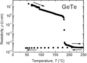
Chalcogenide alloys are a fascinating group of materials that have garnered significant attention for their application in phase change memories (PCM) thanks to their ability to switch between amorphous and crystalline states with the application of heat or electrical current.
Chalcogenide alloys are typically composed of elements from the chalcogen group such as sulfur, selenium, and tellurium, combined with other elements like germanium, antimony, or arsenic and exhibit unique properties that make them ideal for non-volatile memory storage.
This reversible phase transition is accompanied by a dramatic change in electrical resistance, which is exploited to represent binary data. As research and development continue, these materials may pave the way for faster, more efficient, and more durable memory systems, revolutionizing how we store and access information in the digital age.
Chalcogenides containing Ge, Sb, Te and Transition Metal Dichalcogenides (TDMCs) are obtained (at CNR-IMM Rome) by Radio Frequency sputtering: this is a Physical Deposition technique for producing high-quality films on low-temperature substrates.
The technique is cost-effective and flexible, allowing for the deposition of layered materials with precise control over refractive index and thickness.
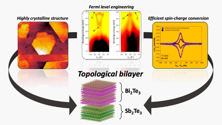
In addition, chalcogenide materials composed of thin films and nanowires of the system (Bi, Sb, Te) can be obtained (in collaboration with CNR-IMM Agrate Brianza) with the MOCVD (metalorganic chemical vapor deposition) synthesis.
MOCVD is a Chemical Deposition technique used to create single or polycrystalline thin films. It can grow crystalline layers to form complex semiconductor multilayer structures.

In MOCVD, ultrapure precursor gases are injected into a reactor. The gases undergo thermal decomposition as they approach the substrate (such as a silicon wafer), leading to the deposition of materials on it. The applications are in the field of devices with properties of PCM, topological insulators (acting as an electrical insulator in its bulk form but allows electrical conduction to occur on its surface, leading to magnetoelectronic and optoelectronic devices) and thermoelectric materials (in which a temperature gradient can lead to the generation of an electric voltage, and conversely, an electric current can induce a temperature gradient).
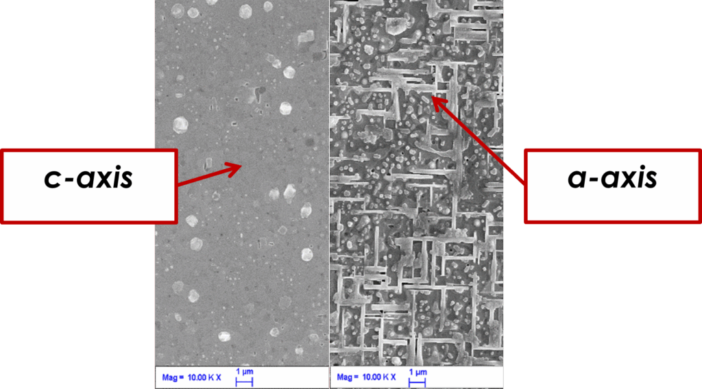
Many analysis tools complement the synthesis of the above materials, including the study of their morphological, structural, compositional and functional properties.
Materials for High Temperature Superconductivity
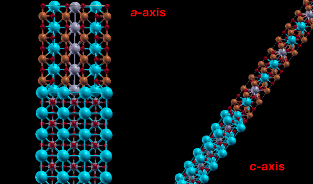
The growth of high-quality epitaxial films of YBa₂Cu₃O₇₋ᵧ (YBCO) is essential for coated conductor (CC) applications. The growth mechanism of YBCO films is strongly influenced by their microstructure, crystallinity, and superconducting properties (https://iopscience.iop.org/article/10.1088/1361-6463/ada3e2, https://iopscience.iop.org/article/10.1088/1361-6463/ad600a, https://iopscience.iop.org/article/10.1088/1361-6668/abb201 , https://ieeexplore.ieee.org/document/8279482 ).

A multiscale modeling approach is adopted, combining experimental structural analysis with ab initio Density Functional Theory (DFT) simulations, to investigate the nucleation and growth of YBCO on reference substrates such as SrTiO₃ and LaAlO₃.
On the experimental side, the impact of the partial pressure of water (PH2O) and the crystallization temperature (Tcryst) on the film microstructure is analyzed through X-ray diffraction, scanning electron microscopy, and critical temperature measurements of films grown by chemical solution deposition using the low-fluorine Metal-Organic Decomposition approach . These techniques demonstrate how the parameters involved during film preparation, namely PH2O and Tcryst, influence interface formation, crystal orientation, and, consequently, the superconducting properties.
From a theoretical perspective, DFT-based calculations are employed to model structural modifications, interface adhesion, and charge transfer at the YBCO/substrate boundary. The work of adhesion (W) determines the nucleation barrier for oriented growth and affects the robustness of the deposition process. This parameter is computed for different surface terminations and substrates relevant to CC manufacturing, in order to identify the most favorable interface configurations. The calculated W value is then incorporated into the proposed kinetic model.
By integrating structural characterization and first-principles calculations, the study provides a fundamental understanding of the chemical pathways governing YBCO film growth. This framework enables the optimization of deposition conditions, promoting the fabrication of high-quality superconducting films for next-generation technological applications.
If this topic is of interest to you, we invite you to visit our vacancies page or drop by one of our offices to discuss it in person!